Wednesday 1 July 2015
Memory and I/O Devices and their interfacing
MEMORY DEVICES
Memory Device Definitions
A device that preserves information for retrieval
Now we see about the basic types of memory components that are commonly used in embedded systems.
We also need to understand the varieties of memory cells that are used to build memories.
There are several varieties of both read-only and read/write memories
After discussing some basic characteristics of memories, we describe RAMs and then ROMs
MEMORY DEVICE ORGANIZATION
The most basic way to characterize a memory is by its capacity, such as 256 MB.
However, manufacturers usually make several versions of a memory of a given size, each with a different data width.
For example, a 256-MB memory may be available in two versions:
■ As a 64M * 4-bit array, a single memory access obtains an 8-bit data item, with a maximum of 2^26 different addresses.
■ As a 32 M *8-bit array, a single memory access obtains a 1-bit data item, with a maximum of 2^23 different addresses.
INTERNAL ORGANIZATION OF A MEMORY DEVICE
The height/width ratio of a memory is known as its aspect ratio.
The best aspect ratio depends on the amount of memory required.
Internally, the data are stored in a two-dimensional array of memory cells as Shown in Figure Because the array is stored in two dimensions , the n-bit address received by the chip is split into a row and a column address (with n=r+c).
A read/write signal (R/W in the figure) on read/write memories controls the direction of data transfer; memory chips do not typically have separate read and write data pins.
Enable pin can be used to easily build large memories from multiple banks of memory chips.
RANDOM ACCESS MEMORIES
Random-access memories can be both read and written. They are called random access because, unlike magnetic disks, addresses can be read in any order.
Most bulk memory in modern systems is dynamic RAM (DRAM).
DRAM is very dense; it does, however, require that its values be refreshed periodically since the values inside the memory cells decay over time.
The dominant form of dynamic RAM today is the synchronous DRAMs (SDRAMs), which uses clocks to improve DRAM performance.
SDRAMs use Row Address Select (RAS) and Column Address Select (CAS) signals to break the address into two parts, which select the proper row and column in the RAM array.
Signal transitions are relative to the SDRAM clock, which allows the internal SDRAM operations to be pipelined.
Timing diagram for a read on a synchronous DRAM
RAS and CAS can therefore become valid at the same time.
SDRAMs use a separate refresh signal to control refreshing.
DRAM has to be refreshed roughly once per millisecond. Rather than refresh the entire memory at once , DRAMs refresh part of the memory at a time.
When a section of memory is being refreshed, it cannot be accessed until the refresh is complete.
The memory refresh occurs over fairly few seconds so that each section is refreshed every few microseconds.
Even faster synchronous DRAMs , known as double-data rate (DDR) SDRAMs or DDR2 and DDR3 SDRAMs, are now in use.
DDRs simply use sophisticated circuit techniques to perform more operations per clock cycle.
SIMMs and DIMMs
Memory for PCs is generally purchased as single in-line memory modules (SIMMs) or double in-line memory modules (DIMMs).
A SIMM or DIMM is a small circuit board that fits into a standard memory socket.
A DIMM has two sets of leads compared to the SIMM’s one.
Memory chips are soldered to the circuit
board to supply the desired memory.
READ-ONLY MEMORIES (ROMs)
Read-only memories (ROMs) are pre programmed with fixed data.
They are very useful in embedded systems since a great deal of the code, and perhaps some data, does not change over time. Read-only memories are also less sensitive to radiation induced errors.
There are several varieties of ROM available.
The first-level distinction to be made is between factory-programmed ROM (sometimes called mask-programmed
ROM) and field-programmable ROM.
Factory-programmed ROMs are ordered from the factory with particular programming.
ROMs can typically be ordered in lots of a few thousand, but clearly factory programming is useful only when the ROMs are to be installed in some quantity.
Field-programmable ROMs, on the other hand, can be programmed in the lab.
Flash memory is the dominant form of field-programmable ROM and is electrically erasable.
Flash memory uses standard system voltage for erasing and programming, allowing it to be reprogrammed inside a typical system.
The flash memory can be reprogrammed while downloading the new memory contents from a telephone line.
Early flash memories had to be erased in their entirety; modern devices allow memory to be erased in blocks.
Most flash memories today allow certain blocks to be protected.
A common application is to keep the boot-up code in a protected block but allow updates to other memory blocks on the device.
As a result, this form of flash is commonly known as boot-block flash.
I/O DEVICES
Some of these devices are often found as on-chip devices in micro-controllers;
others are generally implemented separately but are still commonly used
I/O DEVICES
1.TIMERS AND COUNTERS
2.A/D AND D/A CONVERTORS
3.KEYBOARDS
4.LED’S
5.DISPLAYS
6.TOUCH SCREEN
Timers and Counters
Timers and counters are distinguished from one another largely by their use, not their logic.
Both are built from adder logic with registers to hold the current value , with an increment input that adds one to the current register value.
However, a timer has its count connected to a periodic clock signal to measure time intervals, while a counter has its count input connected to an aperiodic signal in order to count the number of occurrences of some external event.
Because the same logic can be used for either purpose, the device is often called a counter/timer.
WATCH DOG TIMER
A watchdog timer is an I/O device that is used for internal operation of a system.
As shown in Figure ,the watchdog timer is connected into the CPU bus and also to the CPU’s reset line.
The CPU’s software is designed to periodically reset the watchdog timer, before the timer ever reaches its time-out limit.
If the watchdog timer ever does reach that limit, its time-out action is to reset the processor.
In that case, the presumption is that either a software flaw or hardware problem has caused the CPU to misbehave.
Rather than diagnose the problem, the system is reset to get it operational as quickly as possible.
A/D and D/A Converters
Analog/digital (A/D) and digital/analog (D/A) converters (typically known as ADCs and DACs, respectively) are often used to interface non digital devices to embedded systems.
Analog/digital conversion requires sampling the analog input before converting it to digital form.
A control signal causes the A/D converter to take a sample and digitize it.
Keyboards
A keyboard is basically an array of switches, but it may include some internal logic to help simplify the interface to the microprocessor.
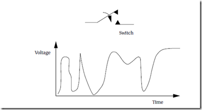
A switch uses a mechanical contact to make or break an electrical circuit.
The major problem with mechanical switches is that they bounce as shown in Figure When the switch is depressed by pressing on the button attached to the switch’s arm, the force of the depression causes the contacts to bounce several times until they settle down.
If this is not corrected, it will appear that the switch has been pressed several times, giving false inputs.
LEDs
Light-emitting diodes (LEDs) are often used as simple displays by themselves, and arrays of LEDs may form the basis of more complex displays.
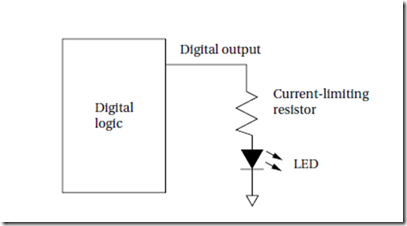
Figure shows how to connect an LED to a digital output.
A resistor is connected between the output pin and the LED to absorb the voltage difference between the digital output voltage and the 0.7 V drop across the LED.
When the digital output goes to 0, the LED voltage is in the device’s off region and the LED is not on.
Displays
A display device may be either directly driven or driven from a frame buffer.
Typically, displays with a small number of elements are driven directly by logic, while large displays use a RAM frame buffer.
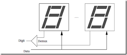
The n-digit array, shown in Figure is a simple example of a display that is usually directly driven.
A single-digit display typically consists of seven segments; each segment may be either an LED or a liquid crystal display (LCD) element.
Touchscreens
A touchscreen is an input device overlaid on an output device.
The touchscreen registers the position of a touch to its surface.
By overlaying this on a display, the user can react to information shown on the display.
The two most common types of touchscreens are resistive and capacitive.
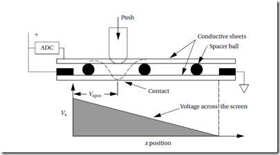
A resistive touchscreen uses a two-dimensional voltmeter to sense position shown in fig.
the touchscreen consists of two conductive sheets separated by spacer balls. The top conductive sheet is flexible so that it can be pressed to touch the bottom sheet.A voltage is applied across the sheet; its resistance causes a voltage gradient to appear across the sheet. The top sheet samples the conductive sheet’s applied voltage at the contact point.
An analog/digital converter is used to measure the voltage and resulting position.
The touchscreen alternates between x and y position sensing by alternately applying horizontal and vertical voltage gradients.
INTERFACING
COMPONENT INTERFACING
Building the logic to interface a device to a bus is not too difficult but does take some attention to detail.
We first consider interfacing memory components to the bus , since that is relatively simple and then use those concepts to interface to other types of devices.
Memory Interfacing
If we can buy a memory of the exact size we need, then the memory structure is simple.
If we need more memory than we can buy in a single chip, then we must construct the memory out of several chips.
We may also want to build a memory that is wider than we can buy on a single chip for example, we cannot generally buy a 32-bit-wide memory chip.
We can easily construct a memory of a given width (32 bits, 64 bits, etc.) by placing RAMs in parallel.
Device Interfacing
Some I/O devices are designed to interface directly to a particular bus, forming glueless interfaces.
But glue logic is required when a device is connected to a bus for which it is not designed.
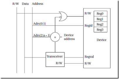
The device has four registers that can be read and written by presenting the register number on the regid pins, asserting R/W as required, and reading or writing the value on the regval pins.
To interface to the bus, the bottom two bits of the address are used to refer to registers within the device, and the remaining bits are used to identify the device itself.
The top bits of the address are sent to a comparator for testing against the device address.
The device’s address can be set with switches to allow the address to be easily changed.
When the bus address matches the device’s, the result is used to enable a transceiver for the data pins. When the transceiver is disabled, the regval pins are disconnected from the data bus.
The comparator’s output is also used to modify the R/W signal: The device’s R/W pin is given the value (bus R/W not-equal address), so that when the comparator’s result is not 1, the device’s R/W pin always receives a 1 to avoid inadvertently writing the device registers.
So in this article i explained about the memory devices , input and output devices and their interfacing.




No comments :
Post a Comment